A NEW WAY TO SEE
Unlocking Deeper Material Insights with Advanced THz Technology
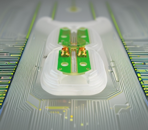
Our unique THz microprobe devices are breaking the limits of conventional THz imaging tools and open a new path to micron-scale resolution contactless near-field measurements.
Learn MoreApplication Areas
Thin-film Inspection 
Contact-less wafer analysis from sheet-resistance to carrier mobility
Contact-less wafer analysis from sheet-resistance to carrier mobility
Terahertz Research 
Get broadband access to THz near-field information
Get broadband access to THz near-field information
Chip Testing 
From chip integrity to fault location
From chip integrity to fault location
Volume Screening 
See micro-defects buried in visually opaque materials
See micro-defects buried in visually opaque materials
Thin-film Inspection
Characterize wafers, solar cells, displays, flexible electronics, and 2D materials (graphene) with non-destructive, contactless probing. Map sheet resistance and carrier mobility at micron-scale resolution.

Terahertz Research
Explore the near-field of metamaterials, plasmonic structures, emitters, waveguides, sensor surfaces, graphene, and more with high-sensitivity, low-invasiveness THz microprobes.

Chip Testing
High-resolution time-domain reflectometry for advanced fault isolation, packaging level inspection, and on-chip THz device characterization. Achieve sub-picosecond resolution with contactless, non-destructive operation.

Volume Screening
Inspect plastic laser welds, fiber-reinforced polymers, organic layers, and more with non-destructive THz imaging. Detect micron-scale defects even in visually opaque materials.

Application highlight
Terahertz On-chip Imaging
A NEW WAY TO SEE: Ultra-fast processes.
Delve into the realm of ultrafast electrodynamics. Discover how real-world phenomena taking place in picoseconds can be visualized using a TeraCube M2 THz near-field imaging system.
A NEW WAY TO SEE: Real-world ultra-fast processes captured with the TeraCube M2.
Recent news
New Milestones First Inline Tool
Product news On-chip THz TDS
From the labs How chiral fermions move
From the labs Chip integrity testing
New Milestones
In a groundbreaking achievement for semiconductor manufacturing, researchers at Samsung Electronics, utilizing key technology from Protemics GmbH, have demonstrated the first-ever use of terahertz near-field microprobes for in-line inspection within a semiconductor fab environment.

From the labs
Researchers from the SKKU and collaborating partners have reported a world-first success in monitoring the spatio-temporal motion of chiral fermions.
From the labs
The Florida Institute for Cybersecurity Research at the University of Florida - a pioneer in the development of new test methods for detecting security-relevant hardware modifications - is now taking chip integrity testing a step further with a TeraCube scanner system.
Products
We develop and manufacture components, sub-systems and full system solutions for high-resolution THz imaging applications.
Click image title on the right for product group details.
© Protemics GmbH
Click image title on the right for product group details.
© Protemics GmbH


People at Protemics


Alexander Michalski Developer
Physicist, developer of data analysis software and optoelectronic systems.

Your Name
Interested in joining our team?

©
2014 - 2026
Protemics GmbH