TeraSpike Defender

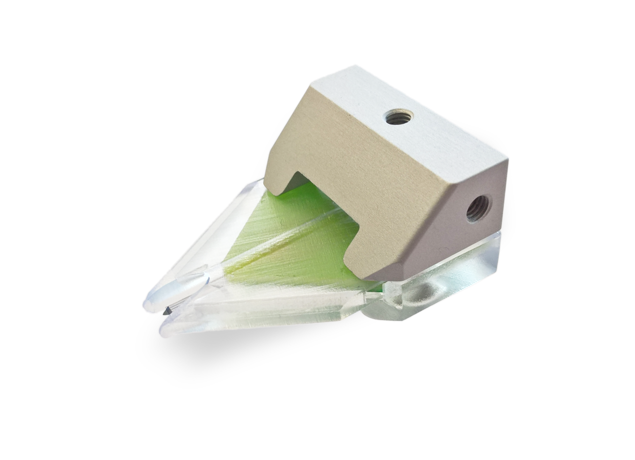
The TeraSpike Defender is an optional housing protecting the sensitive tip of the probe against accidential mechanical impact. The exposure of the tip can be manually adjusted from -1mm to +1mm. In the negative exposure range a direct contact of the probe-tip to a flat surface is prevented by the TeraSpike Defender housing. Optical excitation as well as visual monitoring of the tip region is not impaired by the protective structure thanks to vertically placed openings. The TeraSpike Defender can be applied to any existing or new TeraSpike probe.
SHG-Units

Protemics' SHG-Units offer a user-friendly and highly effective solution to convert femtosecond fiber-laser IR light into NIR light, perfectly suited for the efficient excitation of our LT-GaAs-based TeraSpike microprobes and TeraBlast emitters.
Key benefits:
- Recommended for TeraSpike microprobe operation with IR femtosecond lasers
- High power conversion efficiency
- Passive and robust design
- Short warm-up time(10-15 min)
- Free-space (-FS) and fiber-coupled (-FC) version available
- Easy to use and integrate
Schematic:

Technical specifications:
| Type: TD-1550-SHG | -FS | -MINI-FC |
| Input wavelength range | 1500 .. 1600 nm | |
| Typ. average input power range | 10 .. 200 mW | |
| Typ. power conversion efficiency (a) | 10 .. 50% (a) | |
| Min. aperture diameter | ca. 6 mm | NA |
| Dimension (l x d) | 120 mm x 45 mm | 77 mm x 21 mm |
(a) For an input pulse length of 90 fs and pulse repetition rates of 80 MHz.
For more information please refer to our product brochure (2 MB PDF-file) or contact us.
TeraSpike Phantom

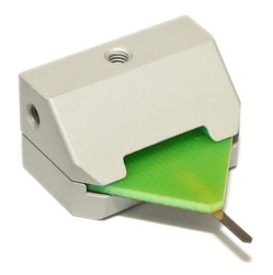
The TeraSpike Phantom is a dummy device for the replacement of a microprobe during construction work and system development. The use of the TeraSpike Phantom - as also included in the starter kit - is recommended to avoid the risk of an uncontrolled mechanical impact in critical working situations.
Accessories
The following accessory is offered.
Connection cable

TS cable
SMP to SMA connection cable plus SMA-to-BNC adapter (also included in the starter kit).
Terahertz Test Target

Target design model: P-TTT-2-1200
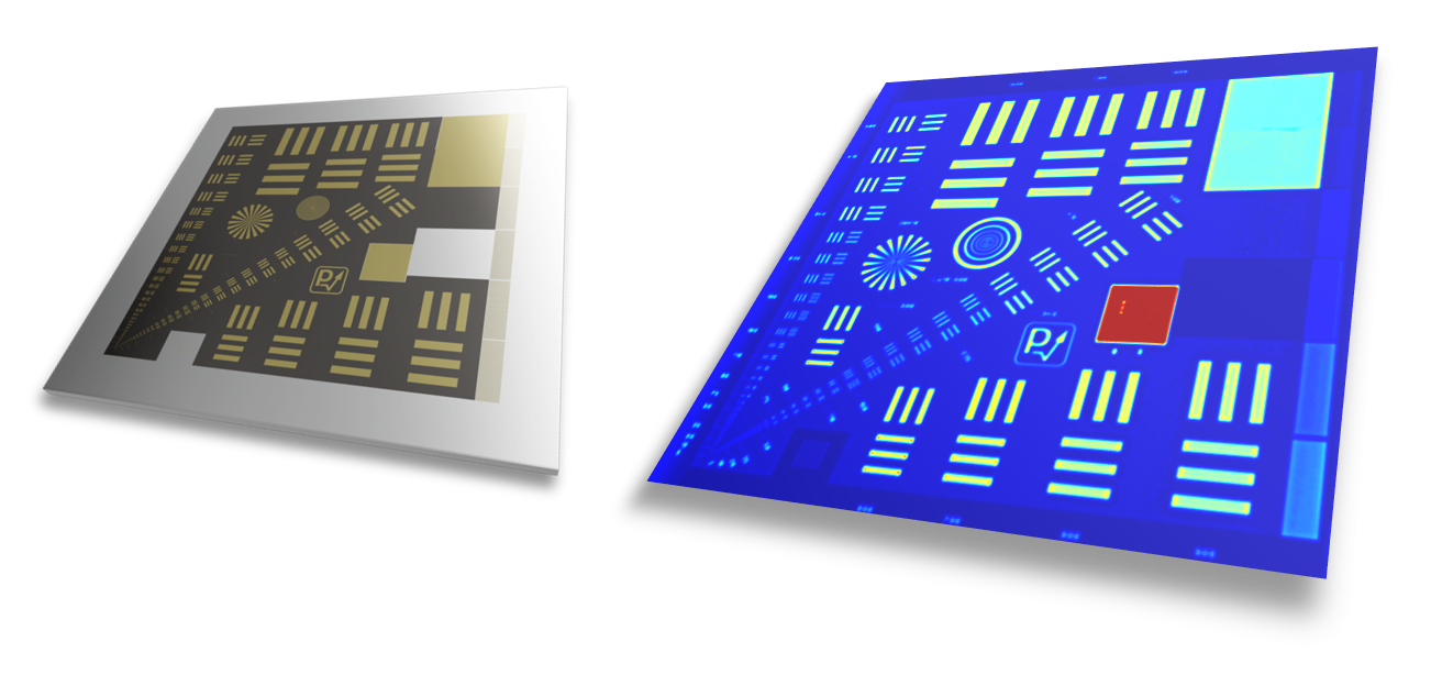
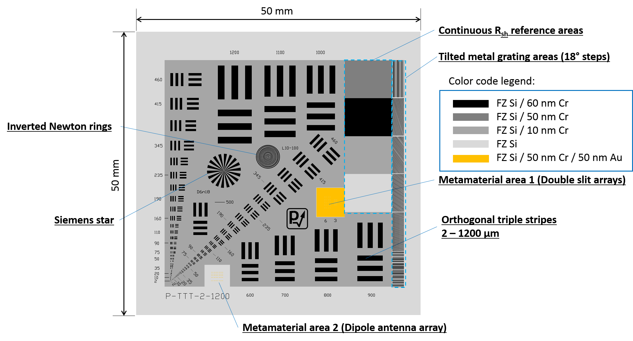
The test target P-TTT-2-1200 has been specially developed for the characterization of Terahertz imaging systems. Featuring structures and areas from 2 µm up to 8 mm of lateral size it is suited for standard diffraction-limited systems as well as near-field imaging systems with sub-wavelength resolution.
The test target is based on high-resistivity silicon and contains conductor areas with three different transmission strengths beside uncoated substrate areas with maximum transmission. The featured structures include classic resolution test structures such as orthogonal pairs of three stripe structures, a Siemens star and concentric rings. These typical structures are accompanied by further structures specially useful for near-field imaging purposes such as metamaterial structures generating local field confinement. Additionally, areas helpful as references for sheet resistance imaging and wafer scanning applications are also listed.
Specifications:

P-TTT-2-1200 |
Value |
|
Substrate material |
High-resistivity FZ silicon, 2-side polished |
|
Substrate Resistivity |
> 10 kOhm cm |
| Target overall size | 2" x 2" (50 mm x 50 mm) |
|
Substrate thickness |
525 µm |
|
Coating materials |
Cr, Au |
|
Coating thickness |
Cr: 10 nm, 50 nm and 60 nm (in semi-transparent areas) Au: 50 nm (opaque) |
|
Orthogonal pairs of three stripe structures |
2 – 1200 µm wide lines & spaces 45° rotated for 2 - 460 µm wide line & spaces |
| Siemens star |
6 mm outer diameter, 18 elements |
| Inverted Newton rings |
5.6 mm outer diameter Ring widths from 10 – 500 µm in increasing steps |
| Continuous Rsh Reference areas |
Four areas, each 6.7 mm x 8.3 mm |
| Tilted metal grating areas |
Six areas, each 2 mm x 6.7 mm Tilting angles: 0°, 18°, 36°, 54°, 72°, 90° |
|
Bow-tie array metamaterial |
300 µm length, 5µm gap |
|
Asymmetric double slit array metamaterial |
3 µm and 6 µm slit width and spaces |